The Tru-SiPh™ Platform advantages stem from five major characteristics. Together, these provide a truly scalable photonic integration platform that can address multiple applications and markets.
Our Fab
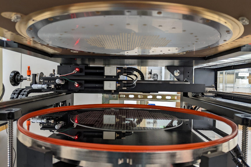
Our devices are fabricated in highly proprietary processes in our Temecula California silicon microstructures foundry. This fab has a 34-year history of providing unique solutions to the silicon and CMOS industry and continues to do so to this day. Using CMOS process tools and unique processes, the Tru-SiPh™ platform is fabricated, tested, and burned-in with a wafer scale process that radically changes the economics of high-performance optics. Our fab also supports integration structures for 2.5D and 3D packaging, useful for higher level integration and copackaged optics. In addition, Skorpios has its own high-volume tools for production of III-V epitaxy.
Proprietary process
Unlike merchant silicon processes squeezed into traditional CMOS fabs, our process for true heterogeneous integration is protected by over 125 worldwide patents (with 25 more pending), and easily twice that number of trade secrets in our own fab. Custom tools have been developed to facilitate our unique process to scale to any reasonable volume.

Platform
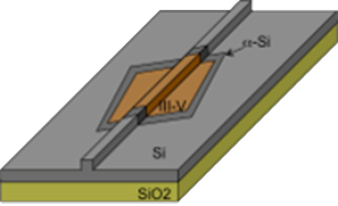
Our thick silicon approach, not available in commercial foundries, provides optics which are inherently insensitive to polarization, provide higher optical confinement and tighter integration with lower losses. Size is further reduced by the integration of lasers and other elements in-plane with the silicon waveguides (rather than glued on top or fiber coupled in separately) and with waveguide fabrication occurring simultaneously on both material systems, no optical alignments are required and extensive reuse of III-V materials within a circuit is possible.
Integration
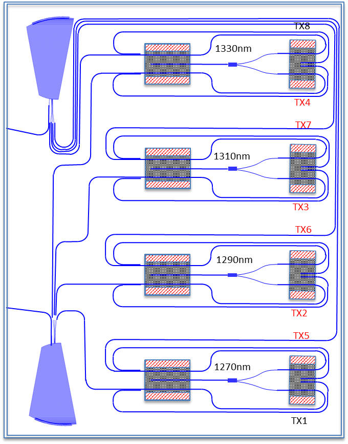
The tight waveguide confinement and embedded epitaxies allow for very high levels of integration in compact form factors for high yield and low cost. The architecture allows each epitaxy to be used for multiple purposes, without additional cost. For instance, SOAs can be simply implemented with lithography on the same piece of epitaxy as the laser.


Wafer scale test and burn-in
Because lasers are incorporated in our structures along with all other optical elements, the photonic circuits can be self-tested. Internal lasers can be monitored with EA modulators or built-in photodiodes. Receivers can be tested with integrated lasers. The entire wafer is tested AND burned-in before die singulation and delivery to the customer, truly a wafer scale process end to end. Built in Self Test (BIST) is a feature of Tru-SiPh™.
Technology Comparison
| Typical III-V Photonics | Typical Si Photonics | Skorpios Si Photonics |
|---|---|---|
|
|
|
| Typical III-V Photonics | Typical Si Photonics | Skorpios Si Photonics |
|---|---|---|
|
|
|
| Typical III-V Photonics | Typical Si Photonics | Skorpios Si Photonics |
|---|---|---|
|
|
|
| Typical III-V Photonics | Typical Si Photonics | Skorpios Si Photonics |
|---|---|---|
|
|
|
| Typical III-V Photonics | Typical Si Photonics | Skorpios Si Photonics |
|---|---|---|
|
|
|
| Typical III-V Photonics | Typical Si Photonics | Skorpios Si Photonics |
|---|---|---|
|
|
|