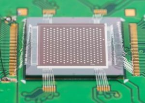
2.5D AND 3D INTEGRATION
Vertical device integration for:
-
Drastically increased performance
-
Shorter critical electrical paths
-
Faster operations on smallest possible footprint
Technology Integration Modules

MEMS
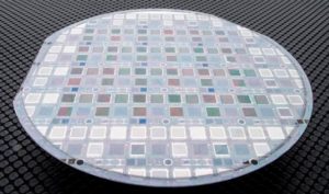
MEMS technologies are often developed on four-inch and six-inch silicon wafers. Skorpios Technologies provides advanced development capabilities on a foundry-compatible eight-inch equipment set, allowing more dies per wafer and lower cost per die. The eight-inch silicon platform enables concurrent integration of MEMS technology with CMOS technology.
Skorpios helps accelerate development and commercialization of MEMS technologies, including:
-
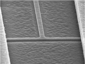
Cantilever-based devices
-
Sealed cavity devices
-
Sensors with high-aspect features
-
Devices with unique material requirements and/or low thermal budgets
MICROFLUIDICS
Microfluidics is a key enabling technology for today’s most innovative lab-on-a-chip (LoC) applications, which are revolutionizing the life sciences industry. Microfluidics technology integrates assay operations like detection, sample pre-treatment, and sample preparation on one chip.
Skorpios helps companies accelerate development and commercialization of LoC products. The technology drivers for these products include nano-scale microfluidic channel sizes, smart sensing, and integration with signal processing — all requiring integration with CMOS.
Sacrificial Materials


SENSORS
Leverage Skorpios’ Integrated Sensor Platform to bond a sensor wafer to CMOS or take advantage of our diverse materials capability to develop a custom sensor that suits your high precision application.
SILICON PHOTONICS
As a critical component of key subsystems in optical network systems, photonic planar lightwave circuits (PLCs) enable superior performance but are challenging and costly to develop and manufacture. By partnering with Skorpios, customers can increase the output of current silicon and quartz-based products, while accelerating the development of new PLC concepts.
Optical waveguide PLC fabrication processes are an extension of CMOS and MEMS processing technology where core lithography, etch, and thin-films technologies apply. Process control of line widths, sidewall roughness, refractive-index uniformity, film thickness, and stress are all key in optimizing device performance.

NOVEL MATERIALS
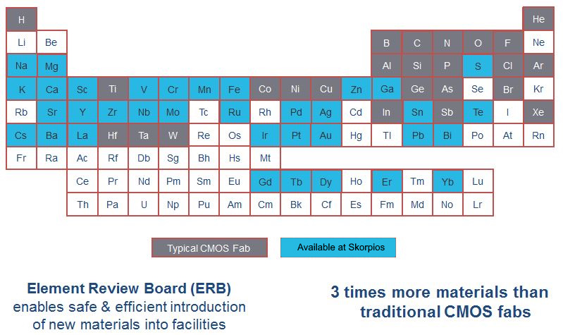
Most CMOS semiconductor foundries can only handle a small selection of materials. Skorpios makes novel materials standard. We utilize an Element Review Board (ERB) to enable safe and efficient introduction of any new materials into our facilities.
